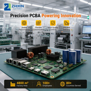
OEM One-Stop PCBA Prototype & Mass Manufacturing
Full turnkey prototype to high-volume SMT/THT assembly. Featuring high-precision component placement, multi-layer stack-ups, and 100% automated optical inspection.

Explore our industrial-grade PCBA portfolio, engineered for mission-critical automotive, smart home, and high-power industrial applications.
Full turnkey prototype to high-volume SMT/THT assembly. Featuring high-precision component placement, multi-layer stack-ups, and 100% automated optical inspection.
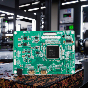
Tailored IoT PCBA manufacturing based on custom Gerber files and BOM lists. Integrated Wi-Fi/BLE modules, low standby power consumption, and conformal coating options.
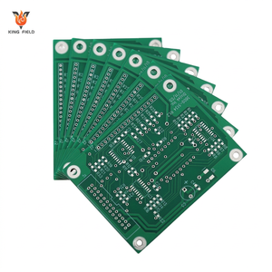
End-to-end bare board fabrication and component integration. Optimized thermal management for high-density micro-via structures and rigid-flex substrates.
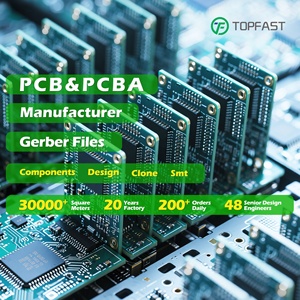
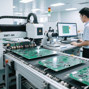
High-speed surface mount technology (SMT) and fine-pitch BGA assembly line capability. Comprehensive DFM testing and rapid NPI turnaround for fast market entry.
Heavy-copper printed circuit board fabrication designed for extreme harsh environments, featuring potted protection, CAN bus communication, and noise immunity.
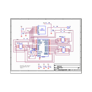
Complete schematic capture, BOM optimization, schematic redesign, and reverse engineering services to upgrade legacy industrial hardware for modern standards.
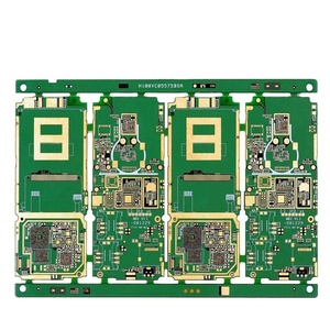
Custom system-on-chip integration, automated in-circuit functional testing (FCT), and advanced firmware flashing for complex automotive & robotic applications.
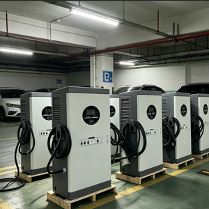
Specialized power electronics board assembly featuring liquid/contact cooling design, planar transformers, and ultra-high voltage isolation for EV fast chargers.
Combining German-engineered quality control standards with agile turnkey PCB contract manufacturing.
From component procurement and raw PCB fabrication to potting, firmware loading, and final enclosure assembly—every step is audited under one unified quality management system.
Equipped with state-of-the-art SMT lines capable of handling 0201 passive components, fine-pitch micro-BGAs, package-on-package (PoP), and heavy copper power layers without bridging.
Implementing 3D Solder Paste Inspection (SPI), Automated Optical Inspection (AOI), X-ray Inspection (AXI), and customized end-of-line functional test systems driven by proprietary software.
Derived from decades of high-reliability German engineering heritage in power conversion and testing infrastructure.

We engineer and assemble high-reliability charger PCBA assemblies used directly on vehicle assembly lines, diagnostic workshops, and fleet management stations worldwide.

Our surface mount and power component integration supports input voltages up to 900V DC. Planar magnetic integration ensures exceptionally high power density in ultra-slim form factors.

Beyond bare PCB soldering, our facility delivers end-to-end mechatronic fabrication. We build turnkey sub-assemblies and market-ready devices packaged for worldwide distribution.
An Industry Whitepaper on Navigating High-Density Interconnects, Power Electronics Integration, and Supply Chain Risk Mitigation.
In today's global market, electronic procurement leaders and hardware design directors no longer search simply for "cheap PCB assembly." Search quality guidelines and empirical procurement data demonstrate a dramatic pivot toward overall value, technical verification, and Information Gain. Buyers seek manufacturing partners capable of mitigating multi-dimensional risks—ranging from component obsolescence and counterfeit active ICs to thermal dissipation bottlenecks in compact enclosures.
Modern Printed Circuit Board Assembly (PCBA) requires absolute convergence between Design for Manufacturability (DFM), Design for Testing (DFT), and robust component sourcing frameworks. Original Equipment Manufacturers (OEMs) across industrial automation, electric vehicles (EV), medical technology, and smart home IoT must evaluate factory capabilities through verifiable quality control benchmarks rather than catalog promises.
Key Procurement Insight: Over 73% of field failures in industrial control boards originate not from raw board fab, but from improper solder paste volume control, undetected BGA micro-cracks, or thermal stress induced during reflow. Partnering with a manufacturer utilizing 3D SPI and AXI inspection eliminates over 99.4% of these latent defects.
As microelectronics shrink while power density demands rise, several critical technical vectors are defining the next decade of PCB fabrication and contract assembly:
A. High-Density Interconnect (HDI) and Micro-Via Architecture: Driven by edge AI computation and 5G communication modules, HDI boards with blind and buried micro-vias have transitioned from high-end consumer mobile phones to standard industrial controllers. Manufacturing facilities must possess high-precision direct laser imaging (LDI) and sequential lamination processes to handle track/space width below 3/3 mil effortlessly.
B. High-Power Density & Advanced Thermal Substrates: The rapid electrification of commercial transport and EV fast-charging networks (30kW to 240kW+) demands PCBA factories capable of working with heavy copper substrates (up to 10oz), insulated metal substrates (IMS/Aluminum boards), and direct bonded copper (DBC). Integrating planar transformers directly into inner board layers allows engineers to replace bulky wire-wound components with ultra-flat, high-efficiency magnetics.
C. Automated Vacuum Potting and Environmental Protection: Industrial electronics deployed in intralogistics, automated guided vehicles (AGVs), and outdoor power stations face constant exposure to severe vibration, humidity, and corrosive atmospheres. Modern assembly plants must integrate multi-axis robotic dispensing systems for silicone, polyurethane, or epoxy encapsulation, ensuring zero-void potting around sensitive components.
D. Traceability, Industry 4.0, and Component Lifecycle Management: Supply chain disruptions have made real-time BOM component auditing imperative. Top-tier assembly facilities utilize MES (Manufacturing Execution Systems) that track every single reel, component lot number, and serial number across SMT placement feeders. If an active component approaches End-of-Life (EOL), proactive engineering teams provide PIN-to-PIN alternative drop-ins during the DFM phase, avoiding costly line stoppages.
To achieve IPC Class 3 compliance (critical for automotive, medical, and aerospace systems where continuous performance or performance-on-demand is imperative), assembly line protocols must adhere to rigorous auditing metrics:
Direct answers to essential technical, engineering, and supply chain queries raised by procurement teams.
Submit your Gerber files, BOM list, and engineering specifications today. Our senior application engineers will provide a comprehensive DFM audit and competitive turnkey quotation.
Get a Quote